DIY Audio Compressor Project
This article will describe an audio compressor which I built recently as a DIY project. The goal was mainly to build an electronic device that will teach me something new rather than to use the compressor for music production.
The article contains requirements for the compressor, design of the electronic circuit, description of how the device has been assembled and tests which I run check the compressor operation.
Prerequisites: The article does not explain what is an audio compressor, basic concepts of electronics, electronic elements and building blocks of electronic circuits that are widely known and their descriptions can be easily found on the Internet.
Acknowledgements: Thank you to Joachim for helping me with this project.
1. Assumptions
Before starting the design I assumed the following characteristics of input signal:
- voltage range - I assumed that voltage range will fit into range from -1V to +1V. I picked this range, because the peak-to-peak voltage measured on my PC was almost 2V.
- frequencies range - humans are able to hear sounds in a frequency range from about 10Hz to 20kHz. Therefore I assumed that frequencies of input signal would be in a range 10Hz-20kHz.
Assumption for the amplifier or other device connected to the compressor’s output:
- input impedance - minimum 1kΩ
- accepts voltage range 5V peak-to-peak
2. Requirements
Following parameters were the required to be present for the compressor:
- release - from 1ms to 1s (later I had to modify the requirement)
- attack - from 0ms to 100ms
- ratio
- threshold
- soft knee and hard knee
- amplifier for compressed signal
I did not specify ranges of values for release, attack, ratio, threshold and amplifier, because my attitude was that I want a minimalistic working device.
Other requirements:
- maximum output voltage - around 5V peak-to-peak
- output impedance is reasonably small
- the input can accept signal of relatively big impedance, say 1kΩ
3. Resources
My design is heavily based on the compressor design presented in these YouTube videos:
I also used the following articles:
4. Electronic design
The high-level idea for the design is that the audio input is buffered and then split into two paths. The first path leads to voltage-controlled amplifier (VCA). The second path processes the input and, according to parameters values, produces a signal that is applied to the VCA and controls whether and if yes, how much, the output from the VCA should be reduced. The compressed signal is then amplified by a parameterized gain and returned as the device output signal. Protection circuit limits signals whose amplitude exceed a maximum predefined level. The diagram below illustrates the compressor design.
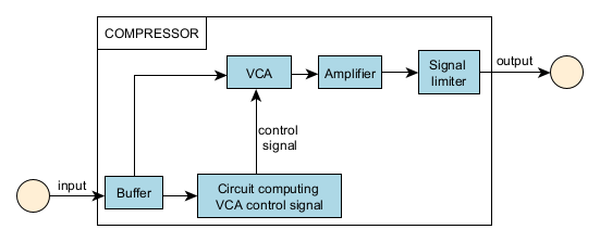
Diagram of high level compressor design
KiCad project of the device with electronic circuit schematic and PCB design is attached here.
4.1. Input buffer
Below picture shows opamp that buffers input signal. The buffered signal is connected to input of VCA and to subcircuit that computes control signal passed to VCA.
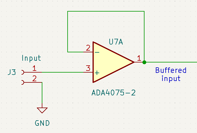
Input buffering
4.2 Determining compressing signal
The subsystem determining compressing signal can be considered a path that starts with an input audio signal and ends with a signal that controls gain of VCA. Subsystem determining compressing signal is comprised of a few logical steps:
- full wave rectification - the input audio signal is converted into its absolute (positive) value.
- envelope detection/peak detection - converts the rectified signal into its envelope. The shape of the envelope depends on values of attack, release and soft/hard knee parameters, which ultimately impacts how quickly the audio signal reduction will be applied and removed.
- subtracting threshold - value of the threshold parameter is subtracted from the envelope. If threshold value is grater than envelope, the step outputs zero.
- signal amplification - the value from the previous step is multiplied by a value dependent on the ratio parameter (for this compressor this value was less than 1) and applied as control signal to VCA.
The diagram below illustrates the process of generating compressing signal.

Determining compressing signal steps
I’ll elaborate on each of the steps to create the VCA controlling signal in the following subsections.
Wave rectification
Below picture shows circuit that performs full wave rectification:

Wave rectification circuit
The circuit is similar to inverting operational amplifier, but a diode is plugged at the opamp’s output. Its operation can be split into two cases:
- The input signal is negative - the opamp will produce positive output and current will flow through the diode similar as in the classical inverting amplifier. Because \(R_{17} = R_{18}\), absolute values of input signal and rectified signal will be equal.
- The input signal is positive - the diode will be reverse biased. Current will not flow through the diode. Thus if the circuit is not loaded, the input signal and rectified signal will be equal. Output of the circuit has impedance equal to \(R_{17} + R_{18}\), so it cannot be connected to a circuit with a low input impedance.
Envelope detection
Below picture shows circuit that performs envelope detection:
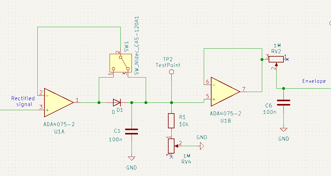
Envelope detection circuit
The circuit begins with a buffer U1A that prevents overloading wave rectification circuit (see previous section). The output of U1A is set according to the rectified signal. Current flowing from U1A’s output loads capacitor C1. The D1 diode prevents current from flowing into the output of U1A. The charge accumulated on C1 is leaked through chain formed by R1 resistor and RV4 potentiometer. RV4 regulates how fast C1 is discharged. This part of the circuit is connected to the buffer U1B, which outputs value equal to voltage at C1 capacitor. This voltage is used to load C6 capacitor through RV2 potentiometer. RV2 regulates how fast C6 is charged. The signal at C6 capacitor will have the shape of the rectified signal envelope.
RV2 potentiometer forms an attack parameter: It determines how fast value of the envelope will rise after the input signal volume increases. The time constant for C6 and RV2 takes values from \(100nF \cdot 0Ω = 0s\) to when RV2 is turned to 0 to \(100nF \cdot 1MΩ = 0.1s\) when RV2 is turned to maximum value. Thus the compressor attack is intended to range from 0s to 0.1s.
RV4 potentiometer forms a release parameter: It determines how fast the value of the envelope will fall after the input signal value decreases. After the input signal value decreases, C1 will be discharged through R1 and RV4. This will result in discharging C6 through RV2 and decreasing envelope signal. Note: In this circuit the RV2 (attack parameter) also impacts how fast the envelope signal decreases. This is not desired, but I decided to accept that. The time constant for C1 and R1 + RV4 takes values from \(100nF \cdot 10kΩ = 0.001s\) to when RV4 is turned to 0 to \(100nF \cdot (10k + 1M)Ω ≈ 0.1s\) when RV4 is turned to maximum value. Thus the compressor release is intended to range from 0.001s to 0.1s (though this time range is impacted by attack subcircuit). Initially I wanted to use 10MΩ potentiometer so release maximum time would be 1s, but I could not find so large potentiometer.
Soft/hard knee is implemented by SW1 switch: Depending of SW1 switch position the buffer U1A feedback loop is wired to the anode or to the cathode side of the diode D1. When the ping 1 of SW1 relays the signal, the feedback in U1A is directly connected to inverting output of U1A. Capacitor C1 will be loaded through diode D1 (soft knee). When the pin 3 of SW1 relays, the feedback in U1A must pass D1. Thus, U1A will output higher voltage and the C1 will be loaded faster (hard knee).
Subtracting threshold
Below picture shows circuit that performs threshold subtraction:

Threshold subtraction circuit
At input the subtraction circuit has a buffer U4A that prevents overloading envelope circuit (see previous section). The signal from the buffer is connected to an inverting summing amplifier U2A modified by addition of diodes D2 and D3.
The second signal that enters the summing amplifier U2A is threshold parameter controlled by RV1 potentiometer. The subcircuit that produces the threshold voltage begins with a voltage reference U3 that outputs 2V. This 2V signal is then inverted by an inverting opamp amplifier to -2V. The RV1 potentiometer converts this voltage to values in range from -2V to 0V.
Operation of U2A can be then split into two cases:
- The envelope plus (negative) threshold is greater than 0: U2A will output negative voltage, the current will flow through D3 and R3. Because U2A outputs negative value and inverting opamp input is 0, D2 diode will be reverse polarized and will not let the current flow. In this scenario U2A operates similar to inverting summing amplifier, though the output at D3 anode will be increased by the diode voltage drop \(V_{out}= - \frac{R_3}{R_5} \cdot V_{env} - \frac{R_3}{R_4} \cdot V_{threshold} + U_{D3} = -V_{env} - V_{threshold} + U_{D3}\)
- The envelope plus (negative) threshold is less than 0: U2A will output positive voltage. D3 will be reverse polarized, so the current will not flow through D3 and R3. Because U2A outputs positive value and inverting opamp input is 0, current will pass through the diode D2 closing the opamp’s feedback loop. The capacitor C2 stabilizes the opamp. Because current does not flow through R3, the circuit output will be the same as inverting input of U2A - 0.
Signal amplification
Below picture shows circuit that performs subtracted feedback amplification:

Signal amplifying circuit
The amplifier takes the subtracted envelope as input. 100kΩ R8 resistor prevents overloading of the subtracting circuit. The signal amplifier is just a standard inverting opamp configuration. Ratio parameter is implemented as RV3 potentiometer. The subtracted envelope is multiplied by a value ranging from 0 (if RV3 is 0Ω) to 1/10 (if RV3 is 10kΩ) and connected to VCA control input. C5 capacitor improves stability of the circuit. I did not determine the range of ratio in the standard way i.e. from 1:M to 1:N, because I did not know what was the exact relation between control signal and VCA’s gain and between envelope produced by the compressor and the actual envelope. This is not entirely correct, but acceptable for me.
4.3 Voltage Control Amplifier (VCA)
Below picture shows VCA circuit:

VCA circuit
Audio input signal is connected at the input of the circuit. C4 removes DC component and R2 converts voltage signal into the current signal (this VCA has a current input signal), which enters the VCA. The signal is then multiplied by a gain (which for this signal range is 1 or less) determined by the circuit from section 4.3. The VCA outputs a current signal that is converted to the voltage signal by U6A opamp.
4.3 End amplifier
Below picture shows circuit that performs amplification of the VCA output and leads signal out of the compressor:

End amplification
The amplifier takes VCA voltage output as input. The signal is amplified by a non-inverting opamp amplifier. End amplification parameter is implemented as RV5 potentiometer. The signal is multiplied by a value ranging from 1 (if RV3 is 0Ω) to 11 (if RV5 is 10kΩ) and connected to the compressor output through resistor R15 which prevents excessive current flowing into the circuit connected to compressor’s output.
4.4 Limiting output signal
Below screen shows circuit that limits signal returned by the compressor:

Signal limitation
The goal of the circuit is to prevent excessive signal volume to be output by the compressor. The circuit takes VCA output amplified by the end opamp. If the magnitude of the signal exceeds 3 diode voltage drops, diodes D11, D10, D9 will conduct current which will limit the signal to 3 diode drops. When diodes D11, D10, D9 open, voltage at the base of Q1 transistor will rise. As a result the transistor will open and LED D5 will start to emit light. Diodes D6, D7, D8 and transistor Q2 operate similarly when magnitude of the signal drops 3 diode voltage drops below 0V. Resistor R15 prevents too big current from flowing through diodes.
When the limit system is on, the compressor output will likely become distorted.
4.5 Selection of electronic components
Active components used for this device are summarized below:
- All operational amplifiers used in this circuit are ADA4075. I chose them because they are widely used, intended for audio-processing circuits and cheap. A single package contains two opamps.
- For Voltage Control Amplifier I chose THAT 2181. Converting voltage signal into current signal at the VCA’s input and converting current signal into voltage signal, values of resistors R11 and R12 is done according to suggested design from the datasheet. The relationship between the gain and the control signal is exponential.
- LM4040 serves as a voltage reference producing 2V at its output.
- Transistors for turning on and off LEDs in limiter are popular BJT transistors BC547B and BC559AP.
All potentiometers used in the device have linear characteristics.
5. Physical assembly of the compressor
5.1 Compressor PCB
I designed PCB of the circuit using KiCad software, ordered manufacturing of the board by JLPC and soldered the board.
Photos below show both sides of the soldered circuit:

One side of the compressor board

Second side of the compressor board
Because of a few issues in the compressor design I had to change some of the board wiring (see kynar wires on the first side of the board). The device has lots of parameters intended to be tunable by its users. Elements that enable this tunability (potentiometers and switches) and limiter circuit LEDs are attached to the device’s case and connected to the board through JST connectors.
For debugging purposes I added a few test points and zero Ohm resistors.
5.2 Compressor casing
I designed the case using FreeCAD software and printed the case using 3D printer (PLA filament). Project file of the case is attached here. The case consists of the actual case and the covering (see screen from FreeCAD below).

Screen of the case project in FreeCAD
The casing has holes for potentiometers, switches, audio and power input/output, LEDs and board holding elements.
5.3 Mounting the board within the case
In the final step I assembled PCB within the casing using a spacer. I mounted connectors, potentiometers, LEDs and switch on the casing side and wired them to PCB. I used cinch connector for audio input and output and GX12 connector for powering. At sides of potentiometers located on the outside of the casing I mounted knobs. Finally I added labels describing what is the purpose of a given element located on the outside of the casing.
Two below photos show the assembled compressor:

Assembled compressor

Front panel of the compressor
This is not particularly ergonomic, but my goal was mainly to learn electronics.
6. Measurements
After assembling the compressor I measured its operation for various parameter values.
I executed measurements using ADP3250 device (it contains oscilloscope and wave generator). As an audio input for all measurements I used a cymbal sound sample imported from a WAV file. Each test was supposed to exercise a single compressor parameter. A test consisted of measurements of compressor input, output and VCA control for two values of a tested parameter (in most cases maximum and minimum values). Compressor was powered from laboratory power supply.
During testing I assumed a default set of values for all parameters. For a single test I changed value of the tested parameter and other parameters were set to their default values. Default values of parameters are as following (though the discrepancy between actual and provided values may be significant):
- attack time - 50 ms
- release time - 500 ms
- soft knee
- threshold - voltage level 0.5 V
- end amplifier - no amplification (gain equal to 1)
- ratio - 0 to 1/10
Obtained results are provided below. Most of diagrams present only the first 200 ms of the input sample.
Attack test
The test checked operation of the attack parameter. Minimum and maximum attack times are 0ms and 100ms respectively. Diagrams below show compressor operation when the attack parameter is set to minimum and maximum values.
Minimum attack

Maximum attack
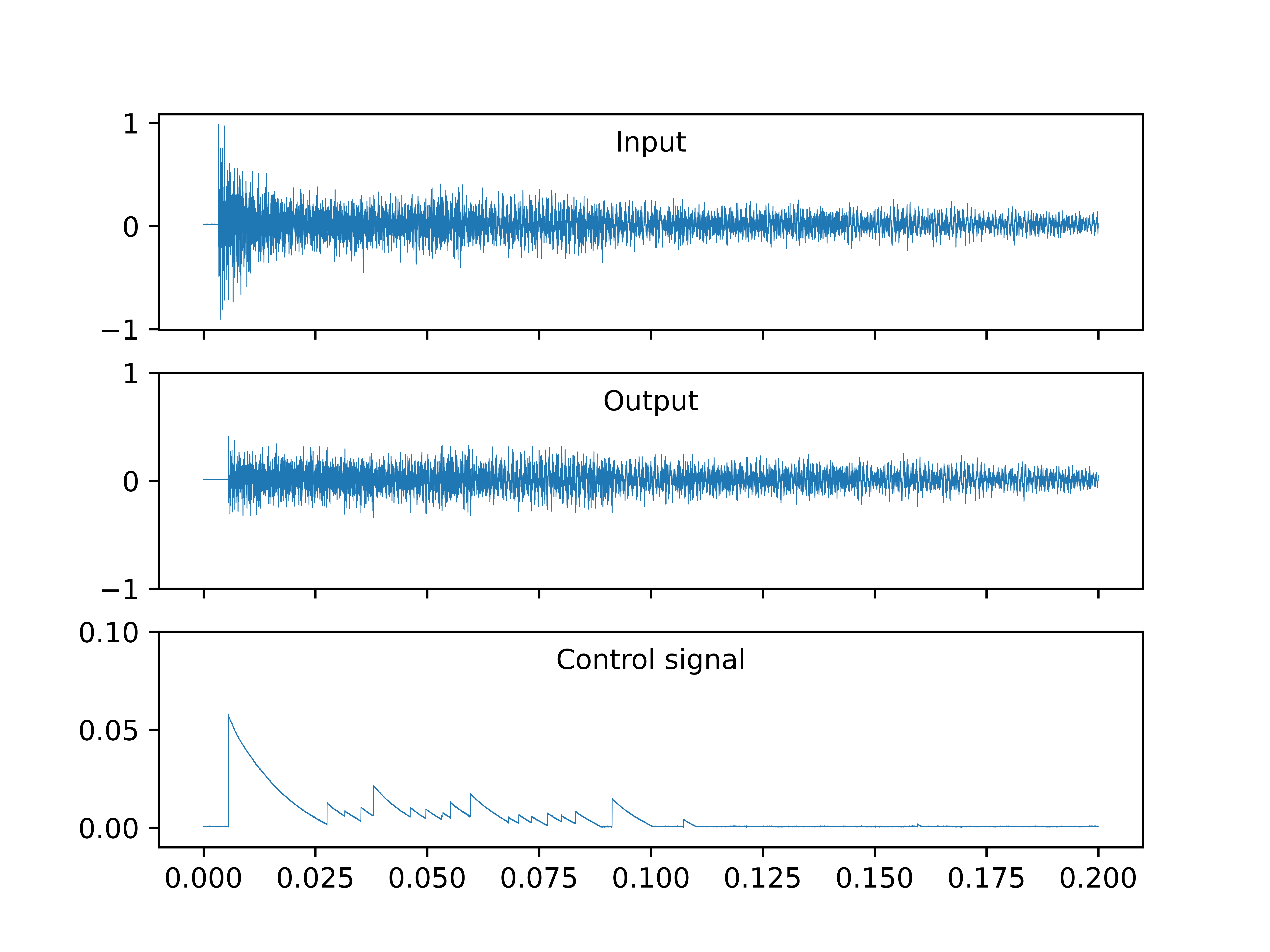
When the attack is set to minimum time, the sound is flattened at the beginning and the control signal rises to around 50 mV at the beginning of the sample.
When the attack is set to maximum time, the sound is not compressed and control signal is zero.
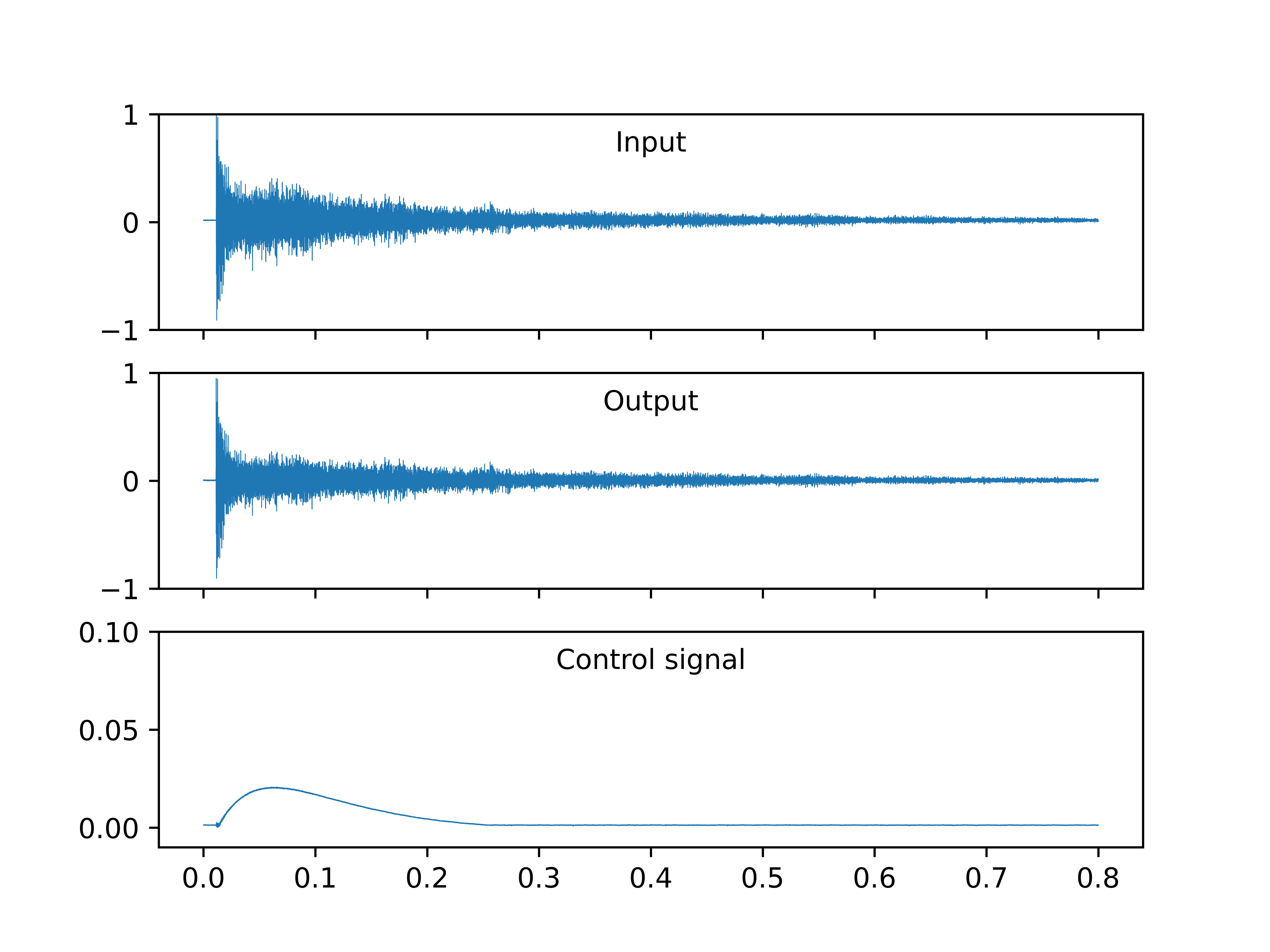
Release test
The test checked operation of the release parameter. Minimum and maximum release time are 1ms and 100ms respectively. Diagrams below show compressor operation when the release parameter is set to minimum and maximum values.

Minimum release

Maximum release
Both for minimum and maximum values of the release parameter the audio is compressed, which is most clearly visible at the beginning of the sample, though they have slightly different shapes. The difference is more apparent in the control signal waveform. For minimum release time control signal consists of many short spikes whereas for maximum release time the signal decreases much less steeply.
Hard/soft knee test
The test checked operation of the hard/soft knee parameter. Diagrams below shows operation of these two knee types.
Soft knee

Hard knee
An error turned up while performing the test. Switching the knee was causing high oscillations that could last a few minutes. Shape of control signal did not differ significantly for these two knee types. Also the control signal shape of both knees differs significantly from control signal shapes obtained during other tests, which is unexpected. My conclusion was that there was an issue with this parameter, but I decided to ignore that. Possible cause was that during knee type switching feedback loop of U1A opamp was disconnected for a short period of time. As a result the opamp produced a large positive or negative voltage. After the feedback is connected again this big voltage is transferred to the capacitor C1 which breaks the envelope generation and possibly disrupts operation of U1A, because of the voltage in the feedback path.
Ratio test
The test checked operation of the ratio parameter. Minimum and maximum ratio values are 0 and 1/10. Diagrams below compare device operation for these two values.
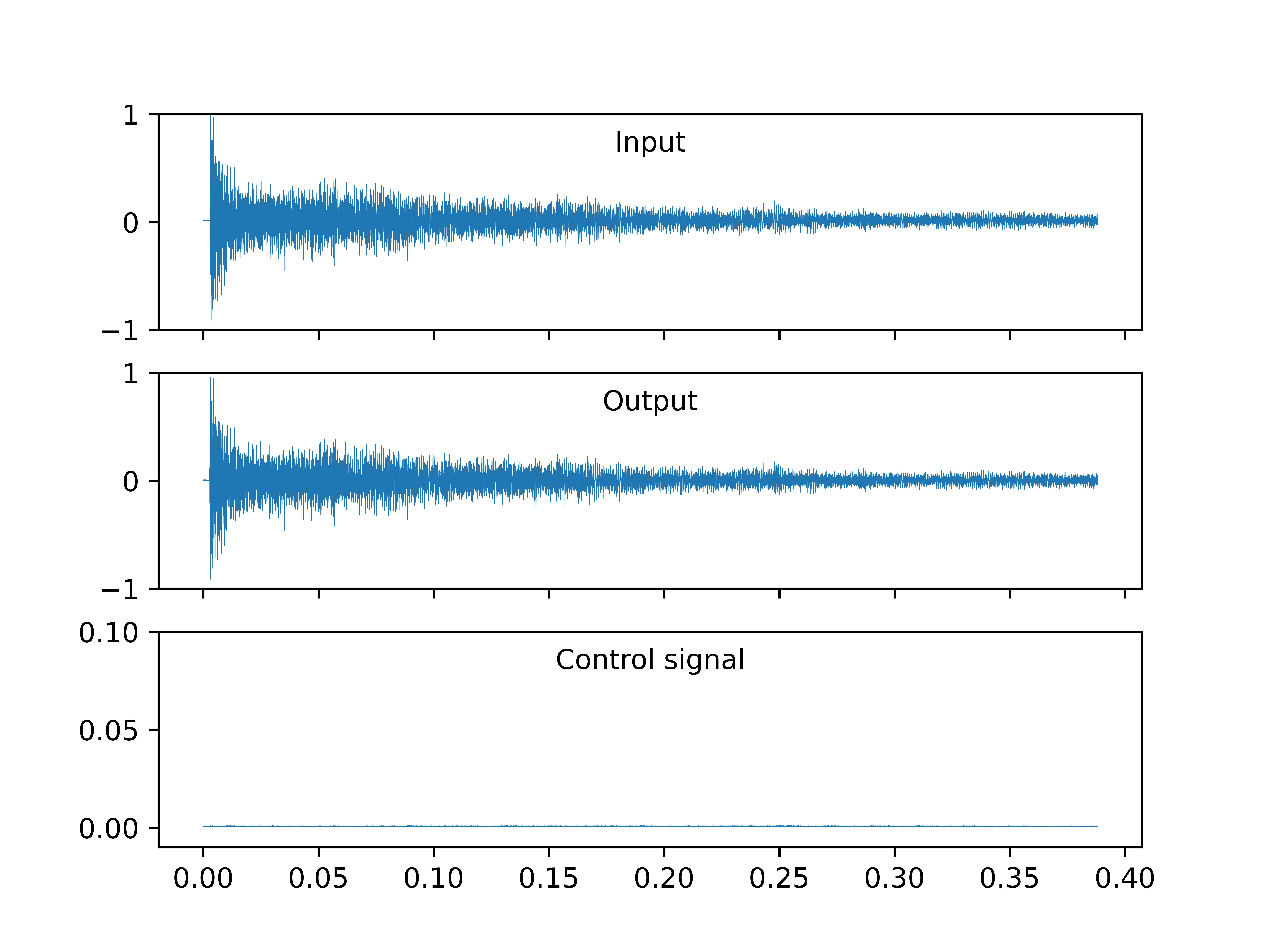
Minimum ratio
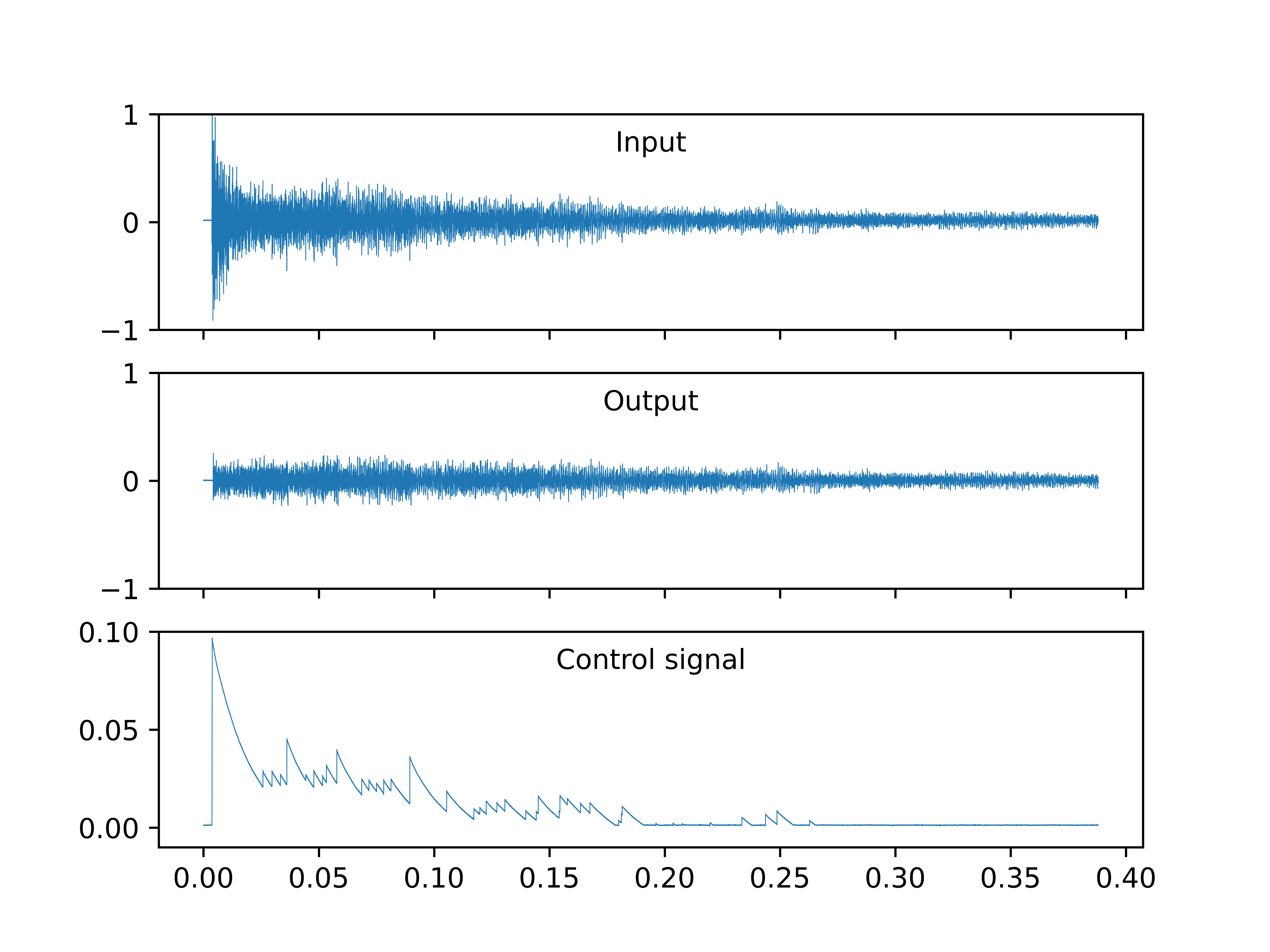
Maximum ratio
When the ratio is set to maximum, the sound is flattened at the beginning and the control signal rises to around 100 mV at the beginning of the sample.
When the attack is set to minimum time, the sound is not compressed and control signal is zero.
Threshold test
The test checked operation of the threshold parameter. Minimum and maximum threshold values are 0V and 2V, though usually users will not know what is the voltage level of their audio signal. Diagrams below compare device operation of minimum and maximum threshold value.

Minimum threshold

Maximum threshold
For the maximum value of the threshold, output signal is slightly reduced compared to the input signal, control signal is slightly greater than 0. Ideally the control signal should be equal to 0 (I assumed that envelope is less than 2V), but such minor reduction was acceptable for me. Note that the control signal is very noisy compared to other tests where control signals drop to 0. I did not investigate this issue. For the minimum value of the threshold the signal is greatly compressed, especially at the beginning of the sample.
Limiter test
The test checked operation of the limiter. To do it I turned end amplification opamp to maximum and turned ratio to minimum so that control signal was 0. Obtained result is shown below.

Limiter
As expected the the output is significantly larger than the input. Maximum level of the output signal is slightly above 2V (which is approximately 3 diode drops that implement the limiter). Also in the first 100ms compressor output does not change significantly whereas in the input signal the sample decreases significantly in this time range. Also LEDs were emitting light during test. These observations confirm that the limiter is working.