DIY Audio Amplifier Project Part I
This post is the first of a two-part series of articles about an audio amplifier I built as a DIY project for the purpose of learning electronics. The post discusses design of electronic circuit of the amplifier. It also discusses simulations and analyses that were run on the KiCad amplifier model to check if the amplifier operation meets expectations. While designing the amplifier I used Audio Power Amplifier Design Handbook as a reference. Most of the ideas used to create the project is taken from this book, although my amplifier is not a direct copy of any amplifier presented there. In the second article I plan to describe the physical construction of the amplifier, process of starting it and its performance.
Prerequisites: The article does not explain basic concepts of electronics, electronic elements and building blocks of electronic circuits that are widely known and their descriptions can be easily found on the Internet.
Caution: If you plan to use this post to built your own amplifier be careful about your speaker and computer (or other equipment) which you connect to the amplifier. If the amplifier draws too big current from the computer, the soundcard may get damaged. Also if the amplifier transmits too much power to the speaker, the speaker may get damaged. Check how much current can be drawn from the soundcard and how much power can be provided to the speaker before connecting the amplifier to it. I give no guarantee that electronic equipment will not break after being connected to the amplifier I present in this article.
Acknowledgements: Thank you to Joachim for helping me with this project.
1. Requirements and assumptions
Before starting the design I set assumptions for input signal and output load (i. e. loudspeaker) parameters:
Input signal:
- voltage range - I assumed that voltage range will fit into range from -0.5V to +0.5V. I picked this range, because it fits consumer line level. However later after designing electrical circuit and creating physical device I measured voltage on minijack on my PC, the peak-to-peak voltage reached almost 2V. This is a different result than what I expected. As a workaround I decided to add a potentiometer in series with the whole amplifier.
- frequencies range - humans are able to hear sounds in a frequency range from about 10 Hz to 20 kHz. Therefore I assumed that frequencies of input signal would be in a range 10Hz-20kHz.
Speaker connected to amplifier:
- input impedance - impedance of the most of loudspeakers is in range from 4Ω to 12Ω. I assumed that impedance of speakers connected to my amplifier will be around 8Ω. Loudspeaker with impedance lower than 8Ω can be connected to the amplifier in series with a resistor of value (8 - loudspeaker resistance)Ω.
- maximum input power - most of loudspeakers can get maximum power value of 10-20W. I assumed that speakers connected to my amplifier can get up to 20W.
I also set requirements for my amplifier:
- power - main goal of audio amplifiers is to increase power of the audio signal. As mentioned before most loudspeakers can get maximum power of 10-20W. I set a requirement that the amplifier should be able to deliver least 15 W to a speaker with input impedance equal to 8Ω.
- voltage gain - The higher the voltage gain, the higher power of the signal. Therefore I decided that the amplifier should increase voltage level of the signal at least by 4.
- variability of voltage gain across signal frequency range - voltage gain should not change much for different frequencies - otherwise sound volume would vary depending on frequency. I did not set precise requirement for maximum change of gain across frequency range. Instead I decided to visually evaluate diagram of amplifier gain in frequency domain. The shape of the curve has to remain flat in the supported frequency range.
- phase shift of the response across signal frequency range - variance of phase shift across frequency range could impact the amplifier sound. Therefore I set a loose requirements, that phase shift should remain as constant as possible within frequency range. Additionally phase shift could matter when connecting feedback loop (described later) - for stability purpose the best option seems to be intuitively to have no phase shift. However I decided not to put any strict requirements on the phase shift and to verify system stability by observing its output.
- shape of output response - amplifier should behave linearly. Input signal within supported range should not cause amplifier saturation.
- input impedance of the amplifier - input impedance should be relatively high to prevent drawing too high current from the input signal source. I assumed that 1kΩ should be enough, although most of commercial amplifiers has higher input impedance e.g. 10kΩ.
2. High level design idea
Audio amplifiers are divided into a few classes. I decided to build an amplifier of class AB, because it is relatively easy to construct as a DIY project and has few disadvantages compared to other classes e.g. class A. My amplifier consists of three main parts: differential pair, cascode and output part. Differential pair and cascode are widely known building blocks of electronic circuits, so this article does not describe their operation (if you do not know how they work - google it). Role of each amplifier part is specified in a separate subsection.
2.1 Differential Pair
Differential pair (also known as long-tailed pair) is the first stage of the amplifier.
Differential pair performs several functions:
- accepts amplifier input - amplifier input is connected to one of differential pair inputs.
- amplifies input by a small factor - further stages have greater gain allowing to reach desired amplification.
- accepts feedback from amplifier output - amplifier output is connected (via capacitor and voltage divider) to one of differential pair inputs. Feedback loop improves stability and linearity of the circuit, although it also limits voltage gain.
- ensures sufficiently high input impedance of the amplifier - the need to have a high input impedance is described in requirements. I did not derive expression for the input impedance, but the simulation results suggested that it should be sufficient.
Differential pair is connected to the cascode amplifier described in the next subsection.
I decided to use a current source at input transistors emitters to improve CMRR (basic version of long-tailed pair has a resistor at input transistors emitters). Also I applied a Wilson current-mirror to split current more equally between the two input transistors.
Reference no 1 in References section is a good source of information about differential pairs.
2.2 Cascode
The second stage of the amplifier is cascode. Its function is to amplify voltage signal coming from the previous stage. Cascode provides the largest part of voltage amplification of all stages. I chose it as a second stage, because of moderately high input impedance and a wide bandwidth. Operating points of cascode transistors are set with voltage divider. Signal from cascode is transmitted to output stage.
2.3 Output stage
Output stage is the final stage of the amplifier. Its main function is to provide high power to the load (i.e. loud speaker). Voltage amplified signal is taken from the previous stage and passed to the load. Output stage enables load to draw sufficiently high current. Therefore it provides a high power to the load (power is product of voltage and current). Apart from supplying sufficient power, the stage has to produce output signal with characteristics of class AB amplifier. That is, operation of output stage should be more efficient than operation of class A amplifier and crossover distortion should not occur as is the case in class B. The stage is implemented as a biased push-pull amplifier. Two complementary Sziklai pairs are components of push-pull pair which alternately turn on and off. I chose Sziklai pairs, because they can supply greater current than a single transistor. Output of this stage is connected to amplifier load. Also, output is connected to the differential pair from the first stage forming feedback loop.
2.4 Simplified schema of the amplifier
To illustrate operation of the amplifier I added its simplified schema. Many elements which are present in the real amplifier are skipped here, because the goal is to demonstrate general operation of the amplifier. Diagram is split by vertical lines into three parts, one for each stage.
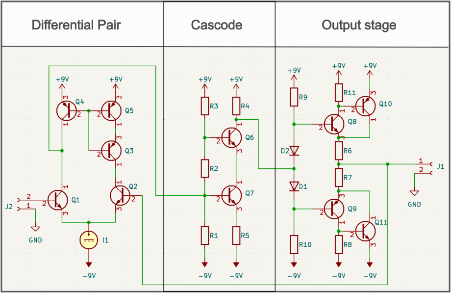
Role of some of the electronic elements from the schema is listed below:
- Differential stage:
- transistor Q1 - takes amplifier input signal
- transistor Q2 - takes feedback loop signal
- transistors Q3, Q4, Q5 - form Wilson current mirror
- Cascode:
- resistors R1, R2, R3 - set operating point of cascode transistors
- transistor Q7 - constitutes common emitter part of cascode
- transistor Q6 - constitutes common base part of cascode
- Output stage:
- diodes D1, D2 - add biasing of push-pull pair
- transistors Q8, Q10 - Sziklai pair in NPN configuration
- transistors Q9, Q11 - Sziklai pair in PNP configuration
3. Electronic design
Electronic design of the amplifier is split into two modules: first module contains a circuit introduced in previous section for amplifying a signal, the second module serves as a power supply. Each module has its own electronic board. Circuits were modeled using KiCad software.
3.1 Details of main amplifier module
This section provides complete electronic design of the amplifier. General idea of amplifier operation and its schema was discussed in the previous chapter, so here I just describe details of the electronic design, which were not provided so far (like usage of additional elements, choosing elements values etc.). KiCad project with electronic circuit schematic and PCB design is attached here.
3.1.1 Differential Pair
Screen of the KiCad model of the subcircuit is provided below.
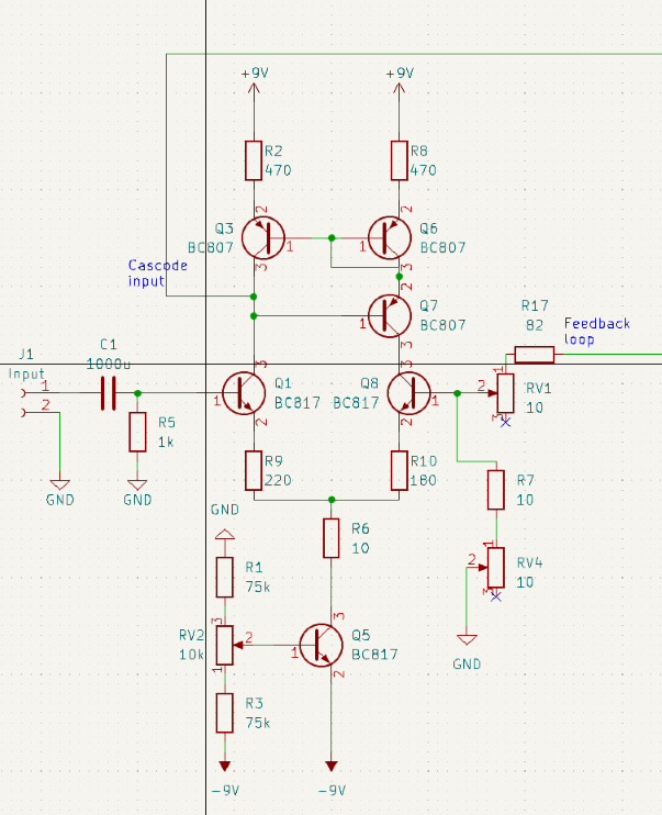
Notes regarding the schema:
- Current source (transistor Q5, resistors R1, R3, potentiometer RV2) - I implemented current source as a transistor biased with two resistors. Additionally there is potentiometer, which can be used to regulate current value.
- Operating point of transistor Q1 - it is set with resistor R5. Current flowing through Q1 is controlled by the current source. For the current to flow through Q1’s collector, Q1’s base also needs to draw current from somewhere. Current cannot be drawn from input since its direct current component is cut off by C1 capacitor. Therefore a resistor connected to ground is added to Q1’s base to enable current flow through the base. A side effect of adding the resistor is a limitation of an input impedance of the amplifier. Too low input impedance could possibly destroy computer network card. Computing the voltage/current ratio of input signal showed that input impedance is around 1kΩ, which hopefully would be sufficiently high.
- Resistors R9 and R10 - these resistors (also called emitter degeneration resistors) constraint differential pair transconductance - differential pair is relatively easy to saturate, so its gain should be kept low. Normally R9 and R10 should have equal values. For some reason unknown to me assigning different values to them finally gave signal amplification on simulation greater than 1 (equal values of R9 and R10 always caused input signal suppression). Different values of emitter degeneration resistors will introduce imbalance to current flowing through Q1, Q8, which contradicts the purpose of Wilson current mirror. However overall circuit produced satisfactory results, so I decided to leave it as it is. Role of emitter degeneration resistors is described in [2].
- Input capacitor C1 - cuts off direct current component of the input signal.
- Voltage divider of feedback loop - direct connecting feedback signal to amplifier did not give good simulation results. I had to calibrate the weight of feedback loop signal by multiplying it by gain (smaller than 1) of voltage divider. It was hard to find resistor values which would give satisfactory amplifier behavior on the simulation, because small changes in resistor values had a big impact on overall response. Finally I managed to find resistor values which gave expected gain and a response shape. However there was no guarantee that the real amplifier would behave exactly the same as the simulation. Therefore I added two potentiometers to enable tuning of feedback signal weight.
3.1.2 Cascode
Screen of the KiCad model of the subcircuit is provided below.
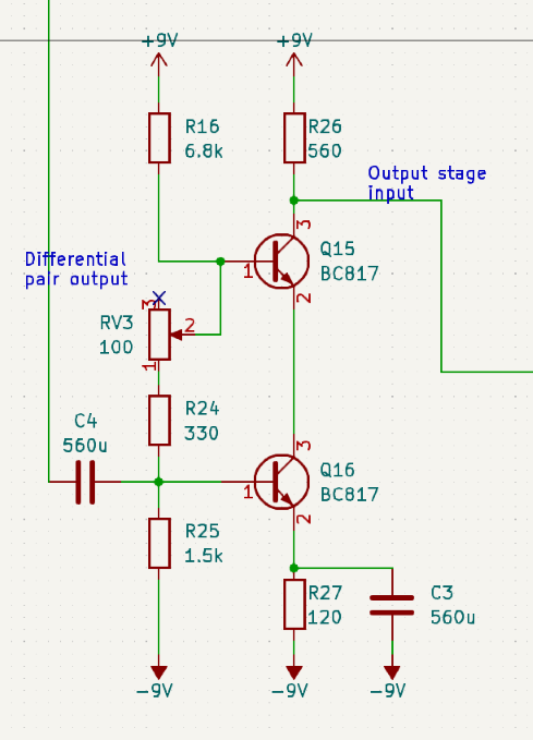
Notes regarding the schema:
- Potentiometer RV3 - voltage amplification of cascode during simulation was satisfactory, but I decided to add possibility to change operating point of cascode transistors in case physical model differs from simulation.
- Connecting output of differential pair and cascode through capacitor C4 - capacitor removes DC component from signal so it does not impact cascode operating point.
- Capacitor C3 - lowers value of Q16 emitter resistance without impacting operating point of transistors. Resistor R27 impacts the operating point of the cascode. For DC current capacitor is a break in the circuit, so C3 does not influence the operating point of the cascode’s transistors. For amplified AC signal C3 is an element with finite impedance. Therefore C3 connected in parallel with R27 lowers Q16 emitter resistance for amplified AC signal, which increases cascode gain.
- Input impedance of cascode - Differential pair has high output impedance, so impedance of C4 (together with whole cascode) should not be too low, because it would disturb operation of differential pair.
3.1.3 Output stage
Screen of the KiCad model of the subcircuit is provided below.
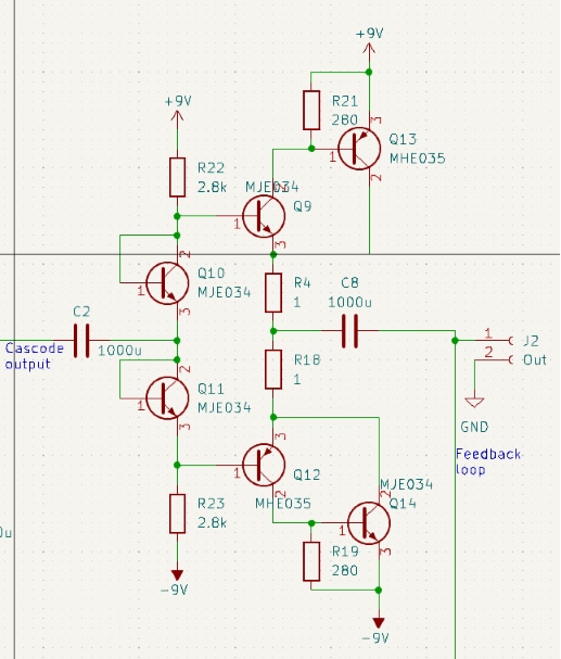
Notes regarding the schema:
- Connecting output stage and output from cascode with capacitor - capacitor cuts DC component from signal so it does not impact output stage operating point.
- Using transistors as diodes (Q10, Q11) - instead of conventional diodes two transistors with bases connected to collectors are used. For some reason implementing diodes with transistors from Sziklai pairs (the same transistor model) gave far better results on simulation than ordinary diodes. I suppose this is because characteristics of such diode configured transistors are similar to characteristics of the first transistors of Sziklai pairs (Q9 and Q12).
- Resistors R21 and R19 - these resistors prevent leakage current and improve turn-off speed of Sziklai pairs. It is described in more detail in [3].
- Connecting output stage and amplifier output with capacitor - capacitor cuts DC component from signal. Only AC current should be provided to a speaker, DC current could break it.
3.2 Powering module
I designed a separate module for powering the amplifier. I chose -9V and +9V to be supply voltages of the amplifier. I decided to use 230V electrical lines for powering (instead of batteries). To make electrical line supply applicable for my device, the powering needed to be converted from 230V AC to -9/+9V DC. Also powering had to be stable. Any voltage spikes from supply module could possibly break electronic elements. KiCad project with the power supply module design is available here.
Screen of KiCad project of the module is provided below:
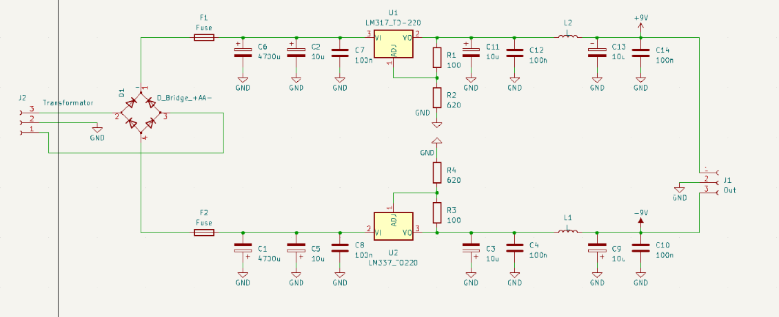
230V electrical line supply is converted to 12V using a transformer (not included on a schema). 12V output from the transformer is connected to J2 connector at the input of the circuit. Next, 12V AC voltage is transferred to diode bridge D1 to perform full-wave rectification. Output signal on pin 1 of diode bridge has positive polarity. The signal passes a fuse F1 protecting from overcurrent. Then there are three capacitors: C6, C2 and C7. Capacitor C6 (electrolytic) flattens the voltage signal from D1. Capacitor C2 (electrolytic) filters noise at low frequencies. Capacitor C7 (ceramic or foil) filters noise at high frequencies. Signal flattened and filtered by capacitors is transmitted to LM317 regulator which aims to produce constant voltage and scales the voltage to be 9V at the regulator’s output (see section 9.3.6 in [4] for the LM317 output computation). Output from LM317 is passed through pi filter to remove any remaining AC ripples. Filtered signal can be then used as a positive voltage supply of the main amplifier board.
Output signal on pin 4 of D1 has negative polarity. Voltage processing is analogous to the processing of voltage with positive polarity. Transformed signal can be then used to as a negative supply of the amplifier board.
4. Simulations
To analyze operation of the amplifier model I run a few types of simulations. Simulations allow to roughly estimate what can be expected from the real amplifier - physical device always differs to some degree from software model, so desired results of simulation do not guarantee desired operation of physical amplifier. Before building the real amplifier I ensured that simulation results meet expectations (some did not, but I decided to skip them). I did not simulate the powering module. Following subsections describe the simulations I run for amplifier along with obtained results.
4.1 Response to a signal of frequency 1kHz and amplitude 0.5V - 1V peak-to-peak
While creating the circuit model I checked its response using SPICE simulation paying attention to gain and shape of the output signal. The default input signal I used during most simulations was a sine wave with frequency equal to 1kHz and amplitude equal to 0.5V. Additionally I run a few tests for input sine waves with different amplitudes and frequencies to ensure correct behavior for various signals.
During designing the amplifier I first simulated behavior of every stage separately and tuned electronic element values to improve output of stages. Next I connected subcircuits into a complete model and checked its behavior. Again, I had to change values of some electronic element values to improve the response gain and its shape.
It was especially difficult to tune resistor values on the feedback loop divider. Changing resistor values of the divider by 1Ω could drastically change the shape of amplifier response (1Ω is often more than tolerance of a resistor!). Also KiCad could give different simulation results after running it multiple times without changing any params. A possible explanation is that there were some errors in KiCad calculations of the response. After some struggle I managed to obtain a satisfactory response.
Following are the voltage gain results provided as amplification factors I got from the final simulation (sine wave, freq=1kHz, amplitude=0.5V): Differential stage: Amplification gain was around 0.5. Amplified was the difference between the input and the feedback loop. The gain was much smaller than required, but was compensated by the later stage. Maximum difference between input and feedback loop was around 40mV and peak-to-peak output signal was around 20mV. Cascode: Amplification gain was around 250. Input signal peak-to-peak value was around 20mV and output signal peak-to-peak value was around 5V. Output stage: Amplification gain was around 0.866. Input signal peak-to-peak value was around 5V and output signal peak-to-peak value was around 4.33V. Whole amplifier: Amplification gain was around 4.33. Input signal peak-to-peak value was 1V and output signal peak-to-peak value was around 4.33V, so the root mean square of the voltage equalled 3.06V.
Load connected to output stage drew 587mA peak-to-peak (root mean square 415mA) . So the power delivered to the load on the simulation computed by multiplying voltage and current root mean squares was 3.06V x 415mA = 1.27W. This was much less then what was in requirements (15W). 1.27W would probably not produce a satisfactory loudness of the speaker. Nonetheless I decided to accept this result, after I was not able to obtain better results within some time.
Below diagram is a screen from SPICE simulation with amplifier output for a sine wave input of frequency 1kHz and 1V peak-to-peak. Time of the simulation was 1ms and step time was 1us.
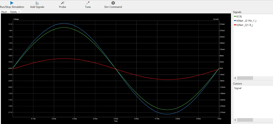
Red line is the voltage value input signal.
Blue line is the voltage value output signal.
Green line is the current value output signal.
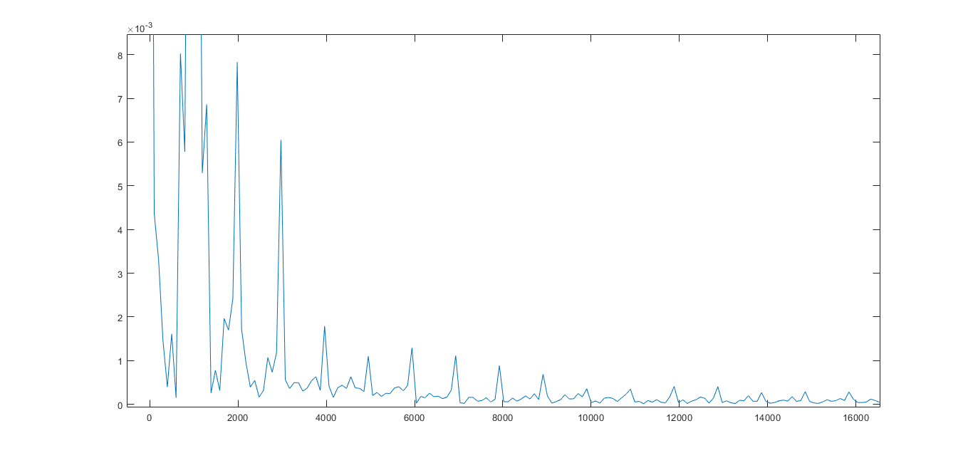
4.2 Total harmonic distortion check
I analyzed the THD of the amplifier output to get information about its harmonic distortions. SPICE and KiCad do not offer functionalities to compute THD, so I used MATLAB for that. I exported amplifier output generated in SPICE simulation. The simulation was run for 10ms with time step of 0.1us for input sine wave input signal with frequency=1kHz and amplitude=0.5V. I wrote a MATLAB script reading exported SPICE data, computing FFT of the signal and drawing it on a plot. From this plot I read the first 20 harmonics and calculated THD using the formula \(THD = \frac{ \sqrt{V_2^2 + V_3^2 + V_4^2 + ... }}{V_1}\) to be around 0.5%. This value was satisfactory for me.
Remark: THD diagram was dependent on simulation time and time step. Too long time step or too short simulation time produced diagrams where no harmonics were visible.
Below diagram shows a fragment of FFT plot of the analyzed amplifier output:
4.3 Frequency analysis
To check amplifier response within supported input signal frequency range I ran a frequency analysis. I computed voltage gain and phase shift of the amplifier output signal for sine waves with amplitude equal to 0.5V and frequency ranging from 5Hz to 200kHz (more than supported frequency range to add some reserve). Both gain and phase shift have change significant at the low frequencies. Gain changes by a factor of around 1.48 between 10 Hz and 30 Hz. Phase shift changes around 73 degrees between 10 Hz and 100 Hz. However apart from these low frequencies gain and a phase shift were relatively constant. These results were satisfactory for me.
Diagram below presents results of the frequency analysis:
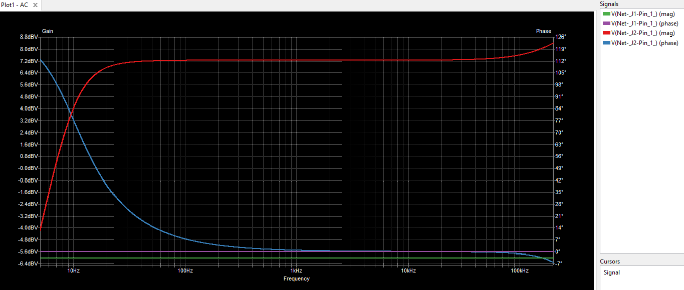
Red line is the voltage value of output signal.
Blue line is the voltage phase shift of output signal.
Green line is the voltage value of input signal.
Purple line is the voltage phase shift of input signal.
5. References
- Paul Horwitz, Winfield Hill, The Art of Electronics, 3rd edition (Cambridge University Press, 2015). Section 2.3.8: Differential amplifiers
- Douglas Self, Audio Power Amplifier Design Handbook, 4th edition (Focal Press, 2006). Chapter 4, Subchapter: Improving input-stage linearity
- Paul Horwitz, Winfield Hill, The Art of Electronics, 3rd edition (Cambridge University Press, 2015). Section 2.4.2 Darlington connection
- LM317 datasheet: https://www.ti.com/lit/ds/symlink/lm317.pdf